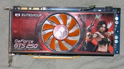
The mid-range graphics discrete accelerator of 2009 with good technical specifications and acceptable performance is the NVidia GeForce GTS 250. The characteristics of this adapter, its capabilities, current cost and user reviews about this solution will be examined in detail.
Graphics adapter niche
The predecessors of this video card can rightfully be considered 8800GTX and 9800GTX. Only now, if these two graphics accelerators belonged to the niche of premium solutions, then the hero of this review was positioned by the manufacturer itself as an average accelerator. At the same time, the level of performance allowed almost all toys to run on PCs equipped with NVidia GeForce GTS 250. Its price was really modest compared to its predecessors.
Graphics chip hardware specifications
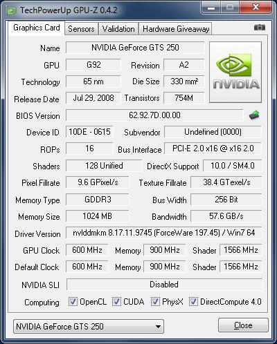
The code name for the NVidia GeForce GTS 250 is G92b. This semiconductor solution included 754 million transistor components and was manufactured to 55nm standards. The graphics accelerator core operated at a frequency of 738 MHz. In this silicon crystal, 128 modules were implemented for processing shaders that operated at a fixed frequency of 1836 MHz. In turn, TMU modules were allocated in the amount of 64 pieces for each conveyor. But such units as ROP, included only 16 pieces in the NVidia GeForce GTS 250. Features the software component of this product indicated full compliance with DX specifications of version 10.0 and support for Open GL technology . The graphics accelerator itself was oriented toward installing in the PCI-E slot 16X version 2.0. There were 3 video outputs for this adapter. One of them output the signal in analog format - it is VGA. Its maximum resolution was declared at the level of 2048rx X 1536rh. And the other two are digital. These included HDMI and, of course, DVI. The latter, in the presence of a special separator, allowed to display the image immediately on 2 monitors. In turn, the maximum resolution for these outputs was 2560x X 1600x.
Heat sink system, temperature and heat pack
The power of this graphics chip was announced at 150 watts. Accordingly, for its full functioning it was necessary to connect an additional connector from the power supply, which compensated for the lack of an additional 75 watts. Also, this value led to the fact that such adapters were equipped with powerful active cooling systems, which occupied 2 expansion slots immediately inside the system unit. The maximum possible temperature value for NVidia GeForce GTS 250 was set at 105 0 . The characteristics of the chip during overclocking indicate that even after overclocking this value does not rise above 75 0 . Therefore, the only case when the temperature of the graphics accelerator is possible up to emergency value, is a breakdown of the cooling system.
Video buffer
NVidia GeForce GTS 250 was aimed at the use of GDDR3 standard microcircuits. Reviews, first of all, highlight the bus width for connecting the video buffer to the GPU, which was equal to 256 bits. Even now, entry-level accelerators in this regard are losing to this "old man" for the reason that they have 128 or 192 bits implemented on the hardware level. The clock frequency of the memory chips was 1100 MHz, and the RAM size in this case could be equal to 512 MB or even 1 GB. As a result, the throughput of the video memory subsystem in this case was 70 GB / s.
Analogs and comparison with them. Test results
The NVidia GeForce GTS 250 graphics card was AMD's main rival to the Radeon HD4770. These adapters had much in common. But the level of performance was significantly better for NVidia products. But energy efficiency is in AMD's solution. The key factor due to which the products of the "red" company won in this case was the manufacturing process. If the GTS 250 chip was produced using the technology of 55 nm, then the AMD - 40 nm. This made it possible to significantly reduce the chip size and power consumption of the adapter. But in gaming applications, the situation was radically different. In the same Crysis with a resolution of 1280x X 1024x and with high settings, the NVidia product could give out 27fps, and AMD - only 24fps. The situation in the Stalker game (Clear Sky version) was a little better for AMD. The GTS 250 in this case could already issue a resolution of 1600px X 1200px and, again, with maximum settings from 13-29fps, and HD4770 - 15-28fps. In any case, the advantage in most toys was more on the side of the old NVidia flagship than AMD's budget solution. But this accelerator was also more affordable in terms of price.
Price and owner reviews
Due to the full sale of existing stocks, it is already impossible to buy the NVidia GeForce GTS 250 in the new state. The price of supported solutions at various online auctions starts at 2,000 rubles for a simplified version with 512 MB. Given that this graphic accelerator will pull GTA V, this is indeed a very modest cost. Also, the bit width of the video buffer bus often appears in reviews, which in this case is equal even to today's standards to fantastic 256 bits. This is the “highlight” that even now allows this accelerator to cope with most of the existing tasks. But still, the era of this accelerator is drawing to a close. Powerful integrated adapters are now appearing, on equal terms with which the hero of this review will soon be unable to compete.
Summary
For its time, the NVidia GeForce GTS 250 was a worthy mid-range accelerator. Its characteristics , as well as test results and owner reviews are another confirmation. And even the mere fact that this product now, even on the most minimal parameters, can pull GTA 5 suggests that it really was a very, very successful video card. But not far off is the moment when, in terms of speed, this product will begin to lose to integrated accelerators. This moment can be considered the end of the era of the GTS 250 and its predecessors, but so far they are still relevant.