In instrumentation and electronics in general, printed circuit boards play a crucial role as carriers of electrical interconnects. The quality of the device and its basic operational characteristics depend on this function. Modern methods of manufacturing printed circuit boards focus on the possibility of reliable integration of the element base with a high density of layout, which increases the working qualities of the manufactured equipment.
PCB Overview
We are talking about products based on a flat insulating base, the design of which has grooves, holes, cutouts and conductive circuits. The latter are used for switching electrical devices, some of which are not included in the device of the board as such, and the other part is placed on it as local functional units. It is important to emphasize that the placement of the above-mentioned structural elements, conductors and working parts is initially presented in the product design as a clearly thought-out electrical circuit. To enable future soldering of new elements, metallized coatings are provided. Previously, copper deposition technology was used to form such coatings. This is a chemical operation that many manufacturers have abandoned today due to the use of harmful chemicals like formaldehyde. It was replaced by more environmentally friendly methods of manufacturing printed circuit boards with direct metallization. The advantages of this approach include the possibility of high-quality processing of thick and double-sided boards.
Materials for the manufacture
Among the main consumables, it is possible to note dielectrics (foil or non-foil), metal and ceramic blanks for the base of the board, insulating gaskets made of fiberglass, etc. The key role in ensuring the necessary operational properties of the product is played not so much by the basic construction materials for the substrates as the outer coatings . The applied method of manufacturing printed circuit boards, in particular, determines the requirements for bonding materials and adhesive coatings to improve adhesion of surfaces. So, epoxy impregnations are widely used for gluing, and polymer varnish compositions and films are used to protect against external influences. As fillers for dielectrics, paper, fiberglass and fiberglass are used. In this case, epoxyphenolic, phenolic and epoxy resins act as a binding component.
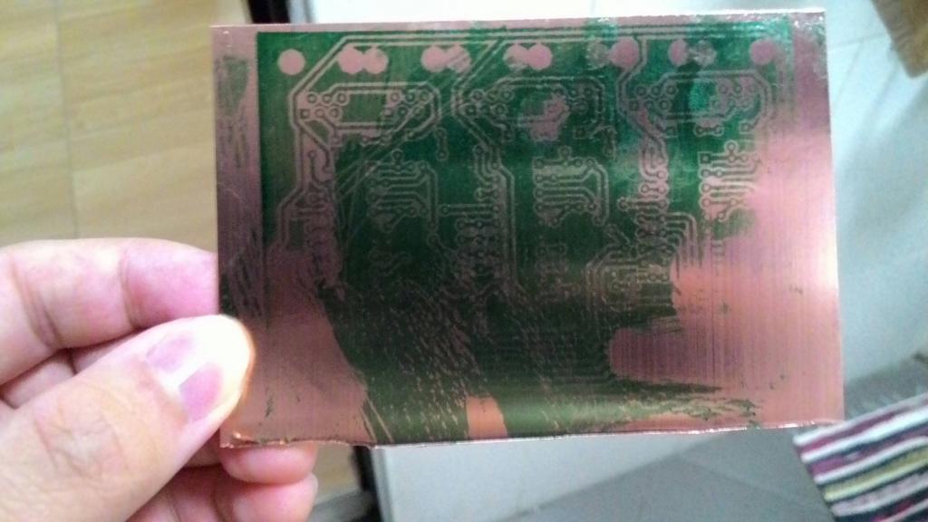
Single-sided printed circuit board manufacturing technology
This manufacturing technique is one of the most common, as it requires minimal resource investment and is characterized by a relatively low level of complexity. For this reason, it is widely used in various industries, where, in principle, it is possible to organize the work of automated conveyor lines for printing and etching. Typical operations of the method of manufacturing single-sided printed circuit boards include the following:
- Preparation of the basics. The workpiece sheet is cut to the desired format by mechanical cutting or stamping.
- The formed package with blanks is fed to the input of the conveyor production line.
- Stripping blanks. Usually performed by mechanical deoxidation.
- Printing inks. Techniques and markings that are resistant to etching and cured by ultraviolet radiation are applied to the screen technology.
- Copper foil etching.
- Peeling off the protective layer.
In this way, low-functional, but cheap boards are obtained. As a consumable, a paper base is usually used - getinax. If the emphasis is on the mechanical strength of the product, then a combination of paper and glass in the form of improved getinaksa brand CEM-1 can be used.
Subtractive manufacturing method
The contours of the conductors of this technique are formed by etching copper foil at the base of the protective image in a metal resist or photoresist. There are various options for implementing subtractive technology, the most common of which involves the use of dry film photoresist. Therefore, this approach is also called the photoresistive method of manufacturing printed circuit boards, which has its advantages and disadvantages. The method is quite simple and in many ways universal, but at the exit from the conveyor boards of small functionality are also obtained. The technological process is as follows:
- A foil dielectric is prepared.
- As a result of layering, exposure and development operations, a protective pattern is formed in the photoresist.
- The process of etching copper foil.
- Removing a protective pattern in a photoresist.
Using photolithography and photoresist, a protective mask is created on the foil in the form of a pattern of conductors. After that, etching is performed in open areas of the copper surface, and the film photoresist is removed.
In an alternative embodiment of the subtractive method of manufacturing printed circuit boards, the photoresist is layered on a foil dielectric, which was previously machined to create holes and preliminary metallization with a thickness of up to 6-7 microns. In areas not protected by photoresist, etching is performed sequentially.
Additive PCB forming technology
Using this method, it is possible to form patterns with conductors and gaps in the range from 50 to 100 microns in width and from 30 to 50 microns in thickness. An electrochemical approach is used with galvanic selective deposition and precision pressing of insulating elements. The fundamental difference between this method and subtractive is that the metal conductors are deposited, not etched. But additive manufacturing methods for printed circuit boards have their own differences. In particular, they are divided into purely chemical and galvanic methods. The chemical method is used more often. In this case, with the formation of conductive circuits in active areas, chemical reduction of metal ions is ensured. The speed of this process is about 3 μm / h.
Positive Combined Manufacturing Method
This method is also called semi-additive. In the work, foil dielectrics are used, but of smaller thickness. For example, a foil of 5 to 18 microns may be used. Further, the formation of a conductive pattern is made according to the same models, but mainly with galvanic deposition of copper. The key difference between the method can be called the use of photo masks. They are used in the combined positive method of manufacturing printed circuit boards at the stage of preliminary metallization up to 6 microns thick. This is the procedure of the so-called galvanic tightening, in which the application and exposure of the photoresistive element through the photomask is performed.
The advantages of a combined method of manufacturing boards
This technology allows you to form drawing elements with increased accuracy. For example, with a positive method of manufacturing printed circuit boards on a foil consumable with a thickness of up to 10 microns, you can get a resolution of conductors up to 75 microns. Along with the high quality of the dielectric contours, a more effective surface insulation with good adhesive ability of the printing substrate is also provided.
Pair pressing method
The technology is based on the technique of making interlayer contacts using metallized holes. In the process of forming the pattern of conductors, sequential preparation of segments of the future foundation is used. At this stage, a semi-additive method of manufacturing printed circuit boards is used, after which a multilayer package is assembled from prepared cores. Between the segments there is a special lining made of fiberglass treated with epoxy resins. When squeezed, this composition can flow out, filling metallized holes and protecting the electroplated coating from chemical attack during further technological operations.
PCB Layering Method
Another method, which is based on the use of several segments of the printed bases to form a complex functional structure. The essence of the method is the sequential superposition of insulation layers with conductors. At the same time, it is necessary to ensure reliable contacts between adjacent layers, which is ensured by galvanic copper build-up in areas with insulating holes. Among the advantages of this method of manufacturing multilayer printed circuit boards, one can note the high density of the arrangement of functional elements with the possibility of compact assembly in the future. Moreover, these qualities are preserved on all layers of the structure. But there are also disadvantages of this method, the main one of which is the mechanical pressure on the previous layers when overlaying the next. For this reason, the technology is limited in the maximum allowable number of layers used - up to 12.
Conclusion
As the requirements for the technical and operational characteristics of modern electronics increase, the technological potential inevitably grows in the tools of the manufacturers themselves. The platform for the implementation of new ideas is often just the printed circuit board. The combined method of manufacturing this element shows the level of modern production capabilities, thanks to which developers can produce ultra-sophisticated radio components with a unique configuration. Another thing is that the concept of layer-by-layer build-up is not always justified in practice of application in the simplest radio engineering, therefore only a few companies are switching to serial production of such boards. Moreover, the demand for simple schemes with a one-sided design and the use of cheap consumables remains.